User talk:Maddie
Carbon Model Development Solutions
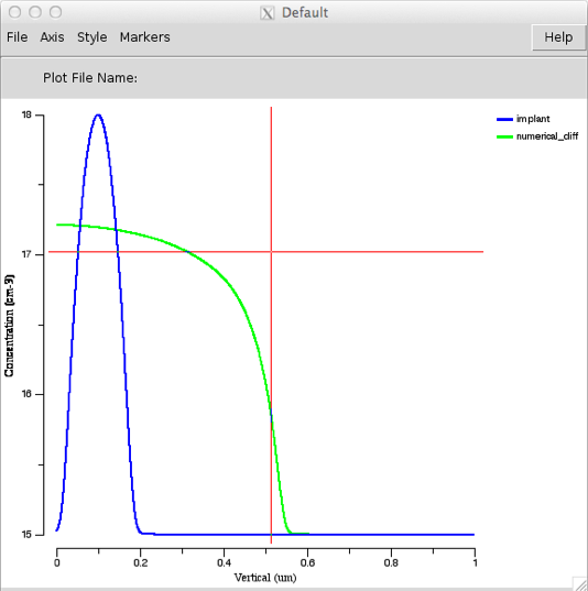
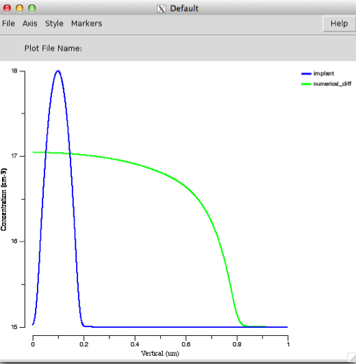
Model Development - simple diffusion Build a simple model for carbon diffusion in silicon. Use a constant diffusivity: Dc = 1.0 * exp(-3.5 / kT) Set the initial carbon profile to: Cc = 1.0e18 * exp(- (x-0.1)*(x-0.1) / 0.001 ) + 1.0e15
Part 1: Diffuse the profile for 60min. at 900, 30min. at 1000, and 10min. at 1100C. Does it agree with what you expect from a simple estimated hand calculation?
Part 2: Modify the model so the diffusivity it proportional to carbon concentration / 1e16 . Run the same anneals – what happens qualitatively?
Results for Part 1:
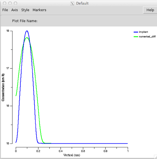
At 900 Celsius for 60 mins:
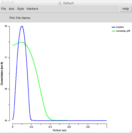
At 1000 Celsius for 30 mins:
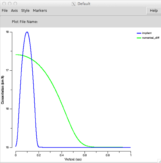
At 1100 Celsius for 10 mins:
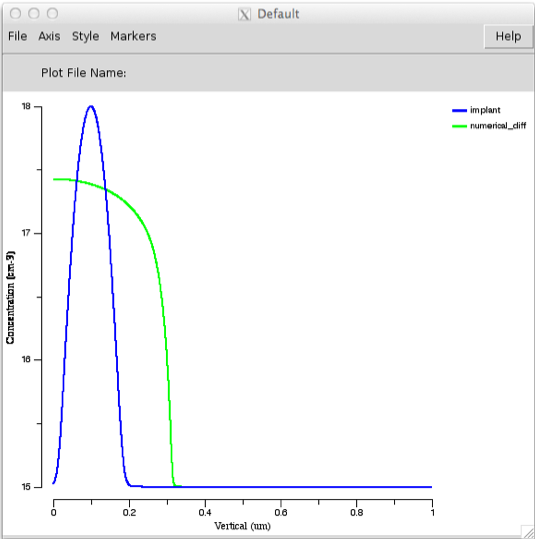
Results for Part 2:
At 900 Celsius for 60 mins:
At 1000 Celsius for 30 mins:
At 1100 Celsius for 10 mins:
Simple Diode I-V Solutions
Diode - simple IV
FIRST: Build a one dimensional silicon diode with a constant p-type doping of 1e16 and an n-type Gaussian w/ peak concentration of 1.0e20 and a junction depth of 0.1um. Think carefully about the grid spacing needed to resolve the problem! Use constant mobility of 1000 for electrons and 200 for holes. Ignore recombination (for now).
CODE:
   #establish diffusion parameters and solution variable "diode"
   DevicePackage
   math diffuse dim=1 umf none col !scale
   solution add name=diode solve !negative
   solution name=Potential nosolve
   solution add name=DevPsi solve negative damp
   solution add name=Elec solve !negative
   solution add name=Hole solve !negative
   pdbSetDouble Silicon diode Abs.Error 1.0e-8
   #absolute error range more important for quasi fermi levels
   pdbSetDouble Silicon diode Rel.Error 1.0e-2
   #establish the grid and assign a material
   line x loc=0.0 spac=0.0002 tag=Top
   line x loc=1.0 spac=0.001 tag=Bottom
   region silicon xlo=Top xhi=Bottom
   init
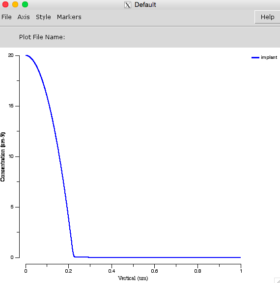
   #Gaussian implant profile
   #fill in the file name for as-implanted profile here
   sel z=1.0e20*exp(-(x)*(x)/(1.086e-3)) name=diode
   #plot the the as-implanted profile
   sel z=log10(abs(diode+1))
   plot.1d label=implant
   #setting the mobility and other variables
   set eps [expr 11.8 * 8.854e-14 / 1.619e-19]
   solution name=qfn add silicon const val= "DevPsi - 0.025*log(Elec/1.0e10)"
   solution name=qfp add silicon const val= "0.025*log(Hole/1.0e10) + DevPsi"
   set Emob "1000.0"; #/ (sqrt(1 + (200*diff(DevPsi)/1.0e7)^2))"
   set Hmob "200.0"; #/ (sqrt(1 + (100*diff(DevPsi)/1.0e7)^2))"
   set T 300.0
   set k 1.38066e-23
   set q 1.619e-19
   set ni "1e10"
   set Na "1.0e16"
   set Nd "10"
   set Vt "[expr {$k*$T/$q}]"
   set ni "1.1e10"
   #continuity equations
   set eqnP "$eps*grad(DevPsi)+Doping-Elec+Hole"
   set eqnE "ddt(Elec)-$Emob*0.025*sgrad(Elec, DevPsi/0.025)"
   set eqnH "ddt(Hole)-$Hmob*0.025*sgrad(Hole, -DevPsi/0.025)"
   pdbSetDouble Si DevPsi DampValue 0.025
   pdbSetDouble Si DevPsi Abs.Error 1.0e-9
   pdbSetString Si DevPsi Equation $eqnP
   pdbSetString Si Elec Equation $eqnE
   pdbSetDouble Si Elec Abs.Error 1.0e-5
   pdbSetString Si Hole Equation $eqnH
   pdbSetDouble Si Hole Abs.Error 1.0e-5
   pdbSetDouble top Hole Abs.Error 1.0e-8
   pdbSetDouble top Elec Abs.Error 1.0e-8
   pdbSetDouble top DevPsi Abs.Error 1.0e-6
   pdbSetDouble top Hole Rel.Error 1.0e-2
   pdbSetDouble top Elec Rel.Error 1.0e-2
   pdbSetDouble top DevPsi Rel.Error 1.0e-2
   pdbSetDouble ReflectBottom Hole Abs.Error 1.0e-8
   pdbSetDouble ReflectBottom Elec Abs.Error 1.0e-8
   pdbSetDouble ReflectBottom DevPsi Abs.Error 1.0e-6
   pdbSetDouble ReflectBottom Hole Rel.Error 1.0e-2
   pdbSetDouble ReflectBottom Elec Rel.Error 1.0e-2
   pdbSetDouble ReflectBottom DevPsi Rel.Error 1.0e-2
   pdbSetBoolean top Elec Fixed 1
   pdbSetBoolean top Hole Fixed 1
   pdbSetBoolean top DevPsi Fixed 1
   pdbSetBoolean top Elec Flux 1
   pdbSetBoolean top Hole Flux 1
   pdbSetBoolean top DevPsi Flux 1
   pdbSetString top Elec Equation {Doping - Elec + Hole}
   pdbSetString top Hole Equation {DevPsi + 0.025*log((Hole+1.0e-10)/1.0e10) - top}
   pdbSetString top DevPsi Equation {DevPsi - 0.025*log((Elec+1.0e-10)/1.0e10) - top}
   pdbSetDouble top Elec Flux.Scale 1.619e-19
   pdbSetDouble top Hole Flux.Scale 1.619e-19
   pdbSetBoolean ReflectBottom Elec Fixed 1
   pdbSetBoolean ReflectBottom Hole Fixed 1
   pdbSetBoolean ReflectBottom DevPsi Fixed 1
   pdbSetBoolean ReflectBottom Elec Flux 1
   pdbSetBoolean ReflectBottom Hole Flux 1
   pdbSetBoolean ReflectBottom DevPsi Flux 1
   pdbSetString ReflectBottom Hole Equation "Doping-Elec+Hole"
   pdbSetString ReflectBottom Elec Equation "DevPsi-0.025*log((Elec+1.0e-10)/1.0e10)"
   pdbSetString ReflectBottom DevPsi Equation "DevPsi+0.025*log((Hole+1.0e-10)/1.0e10)"
   pdbSetDouble ReflectBottom Elec Flux.Scale 1.619e-19
   pdbSetDouble ReflectBottom Hole Flux.Scale 1.619e-19
   line x loc=0.0 spac=.01 tag=Top
   line x loc=0.4 spac=0.001
   line x loc=0.7 spac=0.001
   line x loc=2.0 spac=0.01 tag=Bottom
   region silicon xlo=Top xhi=Bottom
   init
   contact name=top silicon xlo=-0.1 xhi=0.1 add
   contact name=top voltage supply=0.0
   #contact name=GND Silicon xlo=0.9  xhi=1.1 add
   sel z=1.0e21*(x<0.5)-1.0e17 name=Doping
   sel z=0.5*(Doping+sqrt(Doping*Doping+4.0e20))/1.0e10 name=arg
   sel z=0.025*log(arg) name=DevPsi
   sel z=1.0e10*exp(DevPsi/0.025) name=Elec
   sel z=1.0e10*exp(-DevPsi/0.025) name=Hole
   device init; #saves old physics unless you have init
   set plt [CreateGraphWindow]
   contact name=top voltage supply = 1.0
   device time=0.5e-10 movie = {
       set time [simGetDouble Device time]
       set cur [expr ([contact name=top sol=Elec flux] - [contact name=top sol=Hole flux])]
       puts "$time $cur"
       AddtoLine $plt 1.0IV $time $cur
   }
   puts $cur
SECOND:
Implement a simple version of the three device equations and plot current v. voltage. Cut the grid spacing in half, and rerun the current / voltage plot. Does the current change appreciably? What does that say about the choice of grid?
Add a simple SRH recombination with carrier lifetimes of 1 nanosecond. Use 1.0e10 for the intrinsic carrier concentration. How does the reverse bias current change?
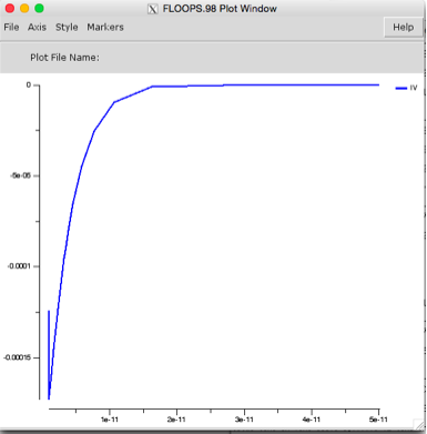
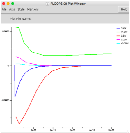
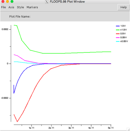
The Implant Profile does not change. However the transient plots are different. In the figures below, the blue lines are the reverse bias voltages. The lighter blue line is a smaller applied reverse bias with magnitude of 0.05 V whereas the darker blue line has a reverse bias magnitude of 1.0 V. In reverse bias, the model with shorter carrier lifetimes will have more recombination current and therefore a larger negative overall current, because more carriers can recombine rather then travel to the other end of the material. The difference between the two figures is difficult to see and the magnitudes of current is extremely small, but Figure 3 has a smaller negative overall current than Figure 2 because of the large difference in carrier lifetimes. After the current has reached its peak, the graph stabilizes to close to zero.
This project also experimented with different hole and electron carrier lifetimes (the lifetimes of the holes and electrons were not equal) and the results of the current versus time plots were similar to the larger lifetime behavior; smaller recombination current. This is believed to be true because its takes both particles to recombine and if some of the particles cannot recombine due to a longer lifetime, then the current of the recombination rate will be smaller, as if both carriers had longer lifetimes.
CODE:
   #establish diffusion parameters and solution variable "diode"
    DevicePackage
    math diffuse dim=1 umf none col !scale
    solution add name=diode solve !negative
    solution name=Potential nosolve
    solution add name=DevPsi solve negative damp
    solution add name=Elec solve !negative
    solution add name=Hole solve !negative
    pdbSetDouble Silicon diode Abs.Error 1.0e-8
   #absolute error range more important for quasi fermi levels
    pdbSetDouble Silicon diode Rel.Error 1.0e-2
   #establish the grid and assign a material
    line x loc=0.0 spac=0.0002 tag=Top
    line x loc=1.0 spac=0.001 tag=Bottom
    region silicon xlo=Top xhi=Bottom
    init
   #Gaussian implant profile
   #fill in the file name for as-implanted profile here
    sel z=1.0e20*exp(-(x)*(x)/(1.086e-3)) name=diode
   #plot the the as-implanted profile
    sel z=log10(abs(diode+1))
    plot.1d label=implant
   #setting the mobility and other variables
    set eps [expr 11.8 * 8.854e-14 / 1.619e-19]
    solution name=qfn add silicon const val= "DevPsi - 0.025*log(Elec/1.0e10)"
    solution name=qfp add silicon const val= "0.025*log(Hole/1.0e10) + DevPsi"
    set Emob "1000.0"; #/ (sqrt(1 + (200*diff(DevPsi)/1.0e7)^2))"
    set Hmob "200.0"; #/ (sqrt(1 + (100*diff(DevPsi)/1.0e7)^2))"
    set T 300.0
    set k 1.38066e-23
    set q 1.619e-19
    set ni "1e10"
    set Na "1.0e16"
    set Nd "10"
    set Vt "[expr {$k*$T/$q}]"
    set ni "1.1e10"
   #SRH Recombination (Simplified) -
    set tau_max_e 1.0e-5
    set tau_max_h 3.0e-6
    set Nref 1.0e16

   #Doping Dependence
    solution name=tau_n add silicon const val= "$tau_max_e/(1+((($Na+$Nd)/($Nref))))"
    solution name=tau_p add silicon const val= "$tau_max_h/(1+((($Na+$Nd)/($Nref))))"
    solution name=SRHrate add silicon const val= "((Elec*Hole)-(1.0e20))/((tau_p*(Elec+$ni))+(tau_n*(Hole+$ni)))"
   #continuity equations
    set eqnP "$eps*grad(DevPsi)+Doping-Elec+Hole"
    set eqnE "ddt(Elec)-$Emob*0.025*sgrad(Elec, DevPsi/0.025)"
    set eqnH "ddt(Hole)-$Hmob*0.025*sgrad(Hole, -DevPsi/0.025)"
    pdbSetDouble Si DevPsi DampValue 0.025
    pdbSetDouble Si DevPsi Abs.Error 1.0e-9
    pdbSetString Si DevPsi Equation $eqnP
    pdbSetString Si Elec Equation $eqnE
    pdbSetDouble Si Elec Abs.Error 1.0e-5
    pdbSetString Si Hole Equation $eqnH
    pdbSetDouble Si Hole Abs.Error 1.0e-5
    pdbSetDouble top Hole Abs.Error 1.0e-8
    pdbSetDouble top Elec Abs.Error 1.0e-8
    pdbSetDouble top DevPsi Abs.Error 1.0e-6
    pdbSetDouble top Hole Rel.Error 1.0e-2
    pdbSetDouble top Elec Rel.Error 1.0e-2
    pdbSetDouble top DevPsi Rel.Error 1.0e-2
    pdbSetDouble ReflectBottom Hole Abs.Error 1.0e-8
    pdbSetDouble ReflectBottom Elec Abs.Error 1.0e-8
    pdbSetDouble ReflectBottom DevPsi Abs.Error 1.0e-6
    pdbSetDouble ReflectBottom Hole Rel.Error 1.0e-2
    pdbSetDouble ReflectBottom Elec Rel.Error 1.0e-2
    pdbSetDouble ReflectBottom DevPsi Rel.Error 1.0e-2
    pdbSetBoolean top Elec Fixed 1
    pdbSetBoolean top Hole Fixed 1
    pdbSetBoolean top DevPsi Fixed 1
    pdbSetBoolean top Elec Flux 1
    pdbSetBoolean top Hole Flux 1
    pdbSetBoolean top DevPsi Flux 1
    pdbSetString top Elec Equation {Doping - Elec + Hole}
    pdbSetString top Hole Equation {DevPsi + 0.025*log((Hole+1.0e-10)/1.0e10) - top}
    pdbSetString top DevPsi Equation {DevPsi - 0.025*log((Elec+1.0e-10)/1.0e10) - top}
    pdbSetDouble top Elec Flux.Scale 1.619e-19
    pdbSetDouble top Hole Flux.Scale 1.619e-19
    pdbSetBoolean ReflectBottom Elec Fixed 1
    pdbSetBoolean ReflectBottom Hole Fixed 1
    pdbSetBoolean ReflectBottom DevPsi Fixed 1
    pdbSetBoolean ReflectBottom Elec Flux 1
    pdbSetBoolean ReflectBottom Hole Flux 1
    pdbSetBoolean ReflectBottom DevPsi Flux 1
    pdbSetString ReflectBottom Hole Equation "Doping-Elec+Hole"
    pdbSetString ReflectBottom Elec Equation "DevPsi-0.025*log((Elec+1.0e-10)/1.0e10)"
    pdbSetString ReflectBottom DevPsi Equation "DevPsi+0.025*log((Hole+1.0e-10)/1.0e10)"
    pdbSetDouble ReflectBottom Elec Flux.Scale 1.619e-19
    pdbSetDouble ReflectBottom Hole Flux.Scale 1.619e-19
    line x loc=0.0 spac=.01 tag=Top
    line x loc=0.4 spac=0.001
    line x loc=0.7 spac=0.001
    line x loc=2.0 spac=0.01 tag=Bottom
    region silicon xlo=Top xhi=Bottom
    init
    contact name=top silicon xlo=-0.1 xhi=0.1 add
    contact name=top voltage supply=0.0
   #contact name=GND Silicon xlo=0.9  xhi=1.1 add
    sel z=1.0e21*(x<0.5)-1.0e17 name=Doping
    sel z=0.5*(Doping+sqrt(Doping*Doping+4.0e20))/1.0e10 name=arg
    sel z=0.025*log(arg) name=DevPsi
    sel z=1.0e10*exp(DevPsi/0.025) name=Elec
    sel z=1.0e10*exp(-DevPsi/0.025) name=Hole
    device init; #saves old physics unless you have init
    set plt [CreateGraphWindow]
    contact name=top voltage supply = 1.0
    device time=0.5e-10 movie = {
        set time [simGetDouble Device time]
        set cur [expr ([contact name=top sol=Elec flux] - [contact name=top sol=Hole flux])]
       puts "$time $cur"
       AddtoLine $plt 1.0IV $time $cur
   }
    puts $cur
   #look into log plots
    device init
    contact name=top voltage supply = -1.0
    device time=0.5e-10 movie = {
       set time [simGetDouble Device time]
        set cur [expr ([contact name=top sol=Elec flux] - [contact name=top sol=Hole flux])]
        puts "$time $cur"
        AddtoLine $plt n1.0IV $time $cur
   }
    device init
    contact name=top voltage supply = 0.5
    device time=0.5e-10 movie = {
       set time [simGetDouble Device time]
        set cur [expr ([contact name=top sol=Elec flux] - [contact name=top sol=Hole flux])]
        puts "$time $cur"
        AddtoLine $plt 0.5IV $time $cur
   }
    contact name=top voltage supply = 0.05
    device time=0.5e-10 movie = {
       set time [simGetDouble Device time]
        set cur [expr ([contact name=top sol=Elec flux] - [contact name=top sol=Hole flux])]
        puts "$time $cur"
        AddtoLine $plt 0.05IV $time $cur
   }
    contact name=top voltage supply = -0.05
    device time=0.5e-10 movie = {
        set time [simGetDouble Device time]
        set cur [expr ([contact name=top sol=Elec flux] - [contact name=top sol=Hole flux])]
        puts "$time $cur"
        AddtoLine $plt n0.05IV $time $cur
   }
