Modeling in one material (e.g. p/n diode, resistor)
Set up governing differential equations in the material:
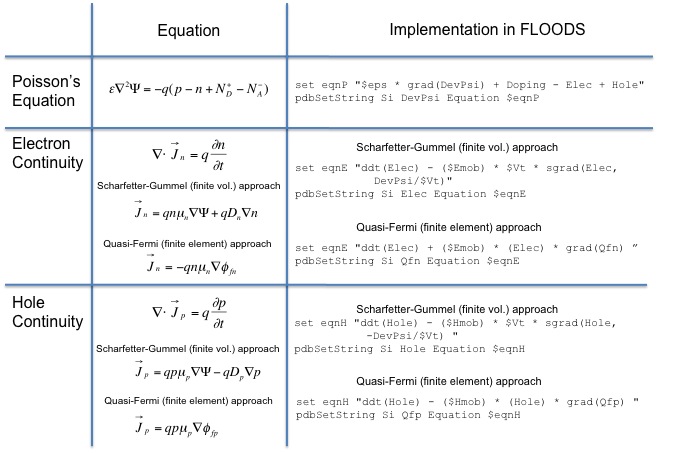
For semiconductors, the basic equations that describe transport of electrons and holes and electrostatic potential are the continuity equations for electrons and holes and the Poisson Equation as given in the table below.
The tcl/alagator scripts for the corresponding differential equations are given in the table, where"eso" is <math>\epsilon_0\epsilon_r/q</math>, "Emob" and "Hmob" are the electron and hole mobilities, and "Vt" is <math>kT/q</math>. One of two approaches may be used to implement the continuity equations (Scharfetter-Gummel or Quasi-Fermi), which use either finite volume or finite element methods, respectively. Note: The Quasi-Fermi representation of current density is simply a transformation (via the Einstein relation and <math>\Phi_{fn}=\Psi-(kT/q)ln(n/n_i)</math>of the independent drift-diffusion representation of the current density \Psi-(kT/q)ln(n/n_i)
Designate solution variables:
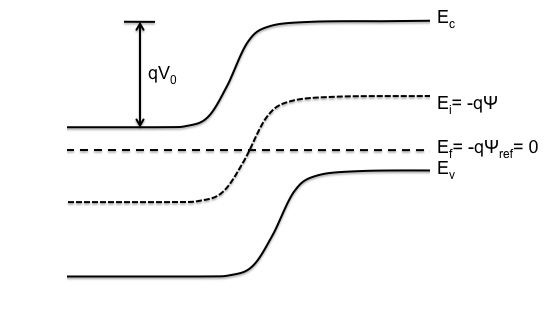
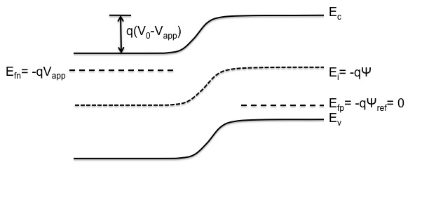
Determine where the reference potential is
Give Boundary Conditions:
Give Initial Conditions:


