PN diode example (1D)
This example builds on the 1D resistor example, showing how to create a floods structure with a doping profile that varies with x. After solving, the example compares floods's numerical results with an analytical solution.
New Concepts
- refining the grid with non-tagged lines
- Doping=f(x) : use "sel z="
- "sel z=" if-then-else syntax (?:)
- tcl "foreach"
1D PN Diode Deck
Create 1D structure - explanation
#Grid
#line x loc=0.0 spac=.01 tag=Top
#line x loc=0.4 spac=0.01
#line x loc=0.7 spac=0.01
#line x loc=2.0 spac=0.05 tag=Bottom
line x loc=0.0 spac=0.1 tag=Top
line x loc=0.5 spac=0.01
line x loc=1.0 spac=0.1 tag=Bottom
mater add name=Silicon
region Silicon xlo=Top xhi=Bottom
init

#Contacts
contact name=VSS Silicon xlo=-0.1 xhi=0.1 add
contact name=GND Silicon xlo=0.9  xhi=1.1 add
Declare solution variables
DevicePackage
solution add name=DevPsi pde solve negative damp
solution add name=Elec   pde solve !negative
solution add name=Hole   pde solve !negative
Define constants
set T 300.0
set k 1.38066e-23
set q 1.619e-19
set Vt [expr {$k*$T/$q}]
set ni 1.1e10
set esi [expr 11.8 * 8.85418e-14]
set eps [expr $esi / $q]
set Emob 350.0
set Hmob 150.0
set small 1.0e-10
Ionized dopant profile - explanation
sel z=1.0e20*(x<0.5) name=Nd
sel z=1.0e17 name=Na
sel z=(Nd-Na) name=Doping
#plot doping
sel z=Doping
plot.1d
#sel z=1.0e20*(x<0.5)-1.0e17 name=Doping
Bulk Equations
set eqnP "$eps * grad(DevPsi) + $Doping - Elec + Hole"
set eqnE "ddt(Elec) - ($Emob) * $Vt * sgrad(Elec, DevPsi/$Vt)"
set eqnH "ddt(Hole) - ($Hmob) * $Vt * sgrad(Hole, -DevPsi/$Vt)"
pdbSetString Silicon DevPsi Equation $eqnP
pdbSetString Silicon Elec   Equation $eqnE
pdbSetString Silicon Hole   Equation $eqnH
pdbSetDouble Silicon DevPsi DampValue $Vt
pdbSetDouble Silicon DevPsi Abs.Error 1.0e-9
pdbSetDouble Silicon Elec   Abs.Error 1.0e-5
pdbSetDouble Silicon Hole   Abs.Error 1.0e-5
Contact Equations
proc OhmicContact {Contact} {
    global Vt ni Nd Na
    pdbSetBoolean $Contact Elec Flux 1
    pdbSetBoolean $Contact Hole Flux 1
    pdbSetBoolean $Contact DevPsi Flux 1
    pdbSetBoolean $Contact Elec Fixed 1
    pdbSetBoolean $Contact Hole Fixed 1
    pdbSetBoolean $Contact DevPsi Fixed 1
    pdbSetDouble $Contact Elec Flux.Scale 1.619e-19
    pdbSetDouble $Contact Hole Flux.Scale 1.619e-19
    pdbSetString $Contact DevPsi Equation "$Nd - $Na - Elec + Hole"
    pdbSetString $Contact Elec Equation "DevPsi - $Vt*log((Elec)/$ni) -$Contact"
    pdbSetString $Contact Hole Equation "DevPsi + $Vt*log((Hole)/$ni) -$Contact"
}
OhmicContact VSS
OhmicContact GND
Initial Conditions - explanation
#Bias contacts
contact name=VSS voltage supply=0.0
contact name=GND voltage supply=0.0
#Initial Guess
sel z= {(Doping>0.0)
            ?  ( 0.025*log( (Doping+$small) / $ni))
            :  (-0.025*log(-(Doping+$small) / $ni))} name = DevPsi
sel z=$ni*exp(DevPsi/$Vt)  name=Elec
sel z=$ni*exp(-DevPsi/$Vt) name=Hole
1st DC Solve at Equilibrium (0V)
device
puts "Electron Flux [contact name=top sol=Elec flux]"
puts "Hole Flux [contact name=top sol=Hole flux]"
#Plot the equilibrium concentration profiles
foreach var {Doping Elec Hole} {
    sel z=log10(abs($var+1.0))
    plot.1d !cle
}
Ramp the DC Bias to make I-V plot
#initialize an array, bias (Vb) and counter (i), and create and new graph window
array set curr {}
set Vb 0.0
set Win [CreateGraphWindow]
set i 1
#Ramp from 0.0-1.2V and Plot
for {set Vb 0.0} {$Vb < 1.2} {set Vb [expr $Vb+0.05]} {
   contact name=top supply = -$Vb
   set Vbias($i) -$Vb
   device init
   set curr($i) [expr ([contact name=top sol=Elec flux] - [contact name=top sol=Hole flux])]
   plot.1d !cle
   AddtoLine $Win IV -$Vb $curr($i)
   incr i
}
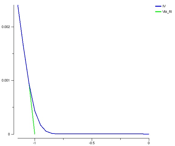
Get the last few points on the IV curve to use for linear extrapolation of the built-in voltage
set l [list "$Vbias(24)" "$curr(24)" "$Vbias(23)" "$curr(23)" "$Vbias(22)" "$curr(22)" ]
Fit the data points with "Bestline". The output will give the x-intercept or built-in voltage
Bestline $l
Create a "fit" line to plot on top of IV curve using the data points and "Bestline" x-intercept result
set line [list "$Vbias(24)" "$curr(24)" "$Vbias(23)" "$curr(23)" "$Vbias(22)" "$curr(22)" 0.9998 0]
CreateSingleLine  $Win Vbi_fit $line
In forward bias (negative voltage applied to the top (n-type) contact), the output IV plot with the absolute value of the built-in voltage equal to 0.9998 is shown below. The built in voltage calculated by the equation Vbi=Vt*ln((Nd*Na)/ni^2) is 0.9786.
