PN diode example (2D): Difference between revisions
Jump to navigation
Jump to search
No edit summary |
No edit summary |
||
| Line 99: | Line 99: | ||
foreach var {Doping Elec Hole} { | foreach var {Doping Elec Hole} { | ||
sel z=log10(abs($var+1.0)) | sel z=log10(abs($var+1.0)) | ||
plot.1d y.v=0.0 !cle | plot.1d '''y.v=0.0 !cle | ||
} | } | ||
Revision as of 02:19, 19 November 2010
New Concepts
- adding another dimension to the structure
- plotting a solution variable in 1d on a 2d structure
1D PN Diode Deck
Create 1D structure - explanation
#Grid
line x loc=0.0 spac=0.1 tag=Top
line x loc=0.5 spac=0.01
line x loc=1.0 spac=0.1 tag=Bottom

line y loc=-1.0 spac=0.1 tag=Lside
line y loc=1.0 spac=0.1  tag=Rside
mater add name=Silicon
region Silicon xlo=Top xhi=Bottom ylo=Lside yhi=Rside
init

#Contacts
contact name=VSS Silicon xlo=-0.1 xhi=0.1 add
contact name=GND Silicon xlo=0.9  xhi=1.1 add
Declare solution variables
DevicePackage
solution add name=DevPsi pde solve negative damp
solution add name=Elec   pde solve !negative
solution add name=Hole   pde solve !negative
Define constants
set T 300.0
set k 1.38066e-23
set q 1.619e-19
set Vt [expr {$k*$T/$q}]
set ni 1.1e10
set esi [expr 11.8 * 8.85418e-14]
set eps [expr $esi / $q]
set Emob 350.0
set Hmob 150.0
set small 1.0e-10
Ionized dopant profile - explanation
sel z=1.0e20*(x<0.5) name=Nd
sel z=1.0e17 name=Na
sel z=(Nd-Na) name=Doping

#plot doping
#sel z=Doping
#plot.1d symb=1
Bulk Equations
set eqnP "$eps * grad(DevPsi) + Doping - Elec + Hole"
set eqnE "ddt(Elec) - ($Emob) * $Vt * sgrad(Elec, DevPsi/$Vt)"
set eqnH "ddt(Hole) - ($Hmob) * $Vt * sgrad(Hole, -DevPsi/$Vt)"
pdbSetString Silicon DevPsi Equation $eqnP
pdbSetString Silicon Elec   Equation $eqnE
pdbSetString Silicon Hole   Equation $eqnH

pdbSetDouble Silicon DevPsi DampValue $Vt
pdbSetDouble Silicon DevPsi Abs.Error 1.0e-9
pdbSetDouble Silicon Elec   Abs.Error 1.0e-5
pdbSetDouble Silicon Hole   Abs.Error 1.0e-5
Contact Equations
proc OhmicContact {Contact} {
    global Vt ni
    pdbSetBoolean $Contact Elec Flux 1
    pdbSetBoolean $Contact Hole Flux 1
    pdbSetBoolean $Contact DevPsi Flux 1
    pdbSetBoolean $Contact Elec Fixed 1
    pdbSetBoolean $Contact Hole Fixed 1
    pdbSetBoolean $Contact DevPsi Fixed 1
    pdbSetDouble $Contact Elec Flux.Scale 1.619e-19
    pdbSetDouble $Contact Hole Flux.Scale 1.619e-19
    pdbSetString $Contact DevPsi Equation "Nd - Na - Elec + Hole"
    pdbSetString $Contact Elec Equation "DevPsi - $Vt*log((Elec)/$ni) -$Contact"
    pdbSetString $Contact Hole Equation "DevPsi + $Vt*log((Hole)/$ni) -$Contact"
}
OhmicContact VSS
OhmicContact GND
Initial Conditions - explanation
#Bias contacts
contact name=VSS voltage supply=0.0
contact name=GND voltage supply=0.0

#Initial Guess
sel z= {(Doping>0.0)
            ?  ( 0.025*log( (Doping+$small) / $ni))
            :  (-0.025*log(-(Doping+$small) / $ni))} name = DevPsi
sel z=$ni*exp(DevPsi/$Vt)  name=Elec
sel z=$ni*exp(-DevPsi/$Vt) name=Hole
1st DC Solve at Equilibrium (0V)
device
puts "Electron Flux [contact name=VSS sol=Elec flux]"
puts "Hole Flux [contact name=VSS sol=Hole flux]"

#Plot the equilibrium concentration profiles
foreach var {Doping Elec Hole} {
    sel z=log10(abs($var+1.0))
    plot.1d y.v=0.0 !cle
}
Ramp the DC Bias to make I-V plot
#initialize an array, bias (Vb) and counter (i), and create and new graph window
array set curr {}
#set Vb 0.0
set i 1

#Ramp from 0.0-1.2V and Plot
set Win [CreateGraphWindow]
for {set bias 0.0} {$bias < 1.2} {set bias [expr $bias+0.05]} {
   set Vbias($i) -$bias

   contact name=VSS supply=-$bias
   device init

   set curr($i) [expr ([contact name=VSS sol=Elec flux] - [contact name=VSS sol=Hole flux])]

   sel z=log10(abs(Hole)+1.0)
   plot.1d !cle

   AddtoLine $Win IV -$bias $curr($i)
   incr i
}

#Get the last few points on the IV curve to use for linear extrapolation of the built-in voltage
set l [list "$Vbias(24)" "$curr(24)" "$Vbias(23)" "$curr(23)" "$Vbias(22)" "$curr(22)" ]

#Fit the data points with "Bestline". The output will give the x-intercept or built-in voltage
Bestline $l

#Create a "fit" line to plot on top of IV curve using the data points and "Bestline" x-intercept result
set line [list "$Vbias(24)" "$curr(24)" "$Vbias(23)" "$curr(23)" "$Vbias(22)" "$curr(22)" -0.99919 0]
CreateSingleLine  $Win Vbi_fit $line
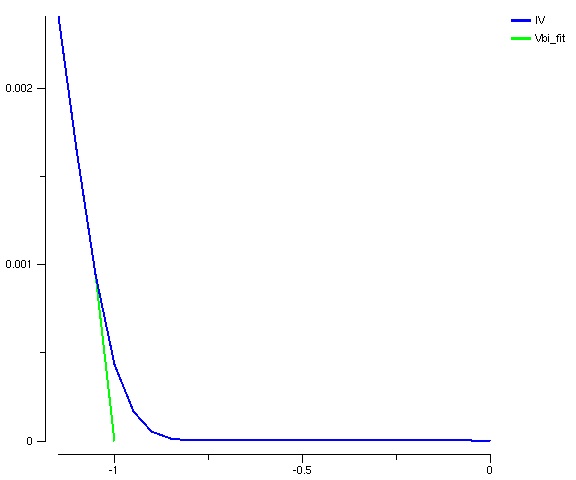
In forward bias (negative voltage applied to the top (n-type) contact), the output IV plot with the absolute value of the built-in voltage equal to 0.9998 is shown below. The built in voltage calculated by the equation Vbi=Vt*ln((Nd*Na)/ni^2) is 0.9786.
Full Deck Without Explanations
Copy-paste this entire deck into a file (for example, 1dpndiode.tcl) to make running it easy. Use the startup script to alias your paths to the floods executable. Then, on the BASH and then flooxs command line type:
$ floods
flooxs> source 1dpndiode.tcl
