High Level Example: p/n Diode: Difference between revisions
No edit summary |
No edit summary |
||
| (4 intermediate revisions by the same user not shown) | |||
| Line 1: | Line 1: | ||
This section provides an overview of all the necessary parts for simulating a p/n diode (in one material) in FLOODS. | This section provides an overview of all the necessary parts for simulating a p/n diode (in one material) in FLOODS. The objective is to familiarize a new user with the physics used in the simulation and how it is implemented in FLOODS. A more detailed, line-by-line, description of the deck for a p/n diode is given in [[Media:[[Example.ogg]]]] | ||
'''Define the Structure''' | '''Define the Structure''' | ||
| Line 51: | Line 51: | ||
solution add name=Hole solve !negative | solution add name=Hole solve !negative | ||
| Line 104: | Line 100: | ||
In this example to forward bias the diode, a positive voltage is applied to the Vcc contact, which is set equal to Qfn by the ohmic contact equations, while GND, which is equal to Qfp, is set to 0V (as seen in the tcl script below). | In this example to forward bias the diode, a positive voltage is applied to the Vcc contact, which is set equal to Qfn by the ohmic contact equations, while GND, which is equal to Qfp, is set to 0V (as seen in the tcl script below). The adjusted band diagram is represented in the figure below. | ||
contact name=Vcc voltage supply=1.0 | contact name=Vcc voltage supply=1.0 | ||
| Line 120: | Line 116: | ||
sel z=0.0 name=Qfn | sel z=0.0 name=Qfn | ||
sel z=0.0 name=Qfp | sel z=0.0 name=Qfp | ||
'''Run the Simulation''' | |||
device | |||
Latest revision as of 16:46, 27 October 2010
This section provides an overview of all the necessary parts for simulating a p/n diode (in one material) in FLOODS. The objective is to familiarize a new user with the physics used in the simulation and how it is implemented in FLOODS. A more detailed, line-by-line, description of the deck for a p/n diode is given in [[Media:Example.ogg]]
Define the Structure
Place lines to designate the top and bottom of the Si diode structure and define the region between the line the be Silicon and then initialize the grid.
line x loc=0.0 spac=0.1*$Mesh_Scale tag=Top
line x loc=1.0 spac=0.1*$Mesh_Scale tag=Bottom
region Silicon xlo=Top xhi=Bottom
init
Define Contacts
contact name=Vcc silicon xlo=-0.1 xhi=0.001 ylo=-1.0 yhi=1.0 zlo=-0.1 zhi=1.1 add
contact name=GND silicon xlo=0.99 xhi=1.1 ylo=-1.0 yhi=1.0 zlo=-0.1 zhi=1.0 add
Establish the doping profile
sel z=1.0e16 name=ND
sel z=1.0e19*(x<0.3)+1.0e10 name=NA
sel z=ND-NA name=Doping
Set up governing differential equations in the material:
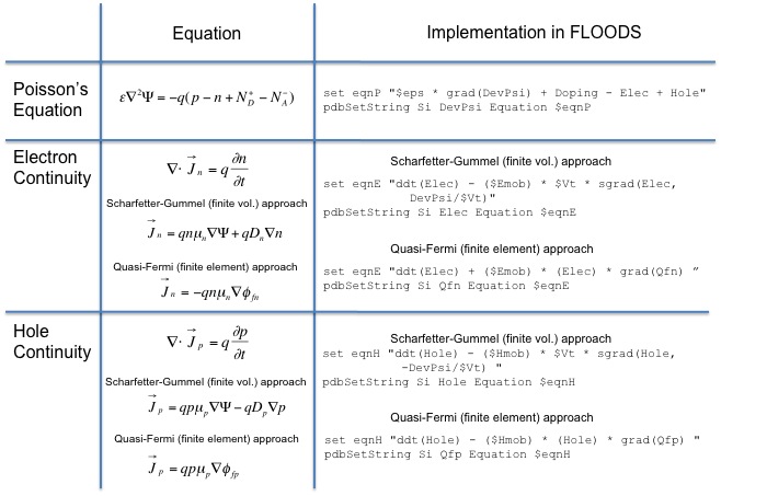
For semiconductors, the basic equations that describe transport of electrons and holes and electrostatic potential are the continuity equations for electrons and holes and the Poisson Equation as given in the table below. Other differential equations such as the heat equation could also be included in the model. The tcl/alagator scripts for the corresponding differential equations are given in the table, where"eso" is <math>\epsilon_0\epsilon_r/q</math>, "Emob" and "Hmob" are the electron and hole mobilities, and "Vt" is <math>kT/q</math>. One of two approaches may be used to implement the continuity equations (Scharfetter-Gummel or Quasi-Fermi), which use either finite volume or finite element methods, respectively.
Determine placement of the reference potential and DevPsi
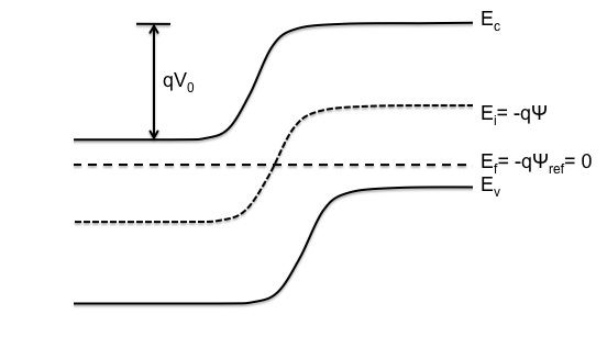
Below is the band diagram of a diode with n-type silicon on the left and p-type silicon on the right.
In order to later set meaningful boundary and initial conditions, the solution variable of electrostatic potential (DevPsi) must be defined in reference to some level. In this case, only one material (silicon) is used in the simulation and thus it is convenient to set the reference potential, or zero, to be the constant Fermi level of the silicon (<math>E_f=-q\Psi_{ref}=0</math>) and DevPsi to be the band-bending at the intrinsic Fermi level (<math>E_i=-q\Psi</math>) of the semiconductor as shown in the figure above. (In other devices that have multiple materials such as a mosfet or heterostructure, it is convenient to set DevPsi to be the band-bending at the vacuum level with reference to the Fermi level.)
- Include discussion of equations for n and p...
Designate solution variables:
If the Sharfetter-Gummel approach is used then the solution variables will be <math>\Psi</math>, n, and p or "DevPsi", "elec", and "hole". They are implemented in FLOODS as follows.
solution add name=DevPsi solve negative damp
solution add name=Elec solve !negative
solution add name=Hole solve !negative
If the Quasi-Fermi approach is used, then the solution variables will be <math>\Psi</math>, <math>\Phi_{fn}</math>, and <math>\Phi_{fp}</math> or "DevPsi", "Qfn", and "Qfp" implemented in FLOODS as follows. In this case, elec and hole need to be defined as constant solution variables.
solution add name=DevPsi solve negative damp
solution add name=Elec const solve val= "$ni*exp((DevPsi-Qfn)/$Vt)+1.0"
solution add name=Hole const solve val= "$ni*exp((Qfp-DevPsi)/$Vt)+1.0"
solution add name=Qfp solve negative damp
solution add name=Qfn solve negative damp
Give Boundary Conditions:
This 1-D device has contacts at the top of the n-type region and the bottom of the p-type region. Thus, boundary conditions need to be specified at those places only. You will need three equations for the three solution variables.
The following script sets ohmic boundary conditions for solution variables, elec , hole, and DevPsi (using Scharfetter-Gummel approach). It establishes conservation of charge ("ND - NA - Elec + Hole"=0) and the quasi-Fermi potentials to be equal to the contact potential, or applied potential though the equation for electron or hole concentration. The word "contact" would be replaced by the contact name (e.g. Vcc or GND) as defined in the Contact section.
pdbSetBoolean $Contact Elec Flux 1
pdbSetBoolean $Contact Hole Flux 1
pdbSetBoolean $Contact DevPsi Flux 1
pdbSetBoolean $Contact Elec Fixed 1
pdbSetBoolean $Contact Hole Fixed 1
pdbSetBoolean $Contact DevPsi Fixed 1
pdbSetDouble $Contact Elec Flux.Scale 1.619e-19
pdbSetDouble $Contact Hole Flux.Scale 1.619e-19
pdbSetString $Contact DevPsi Equation "ND - NA - Elec + Hole"
pdbSetString $Contact Elec Equation "DevPsi - $vt*log((Elec)/$ni) -$Contact"
pdbSetString $Contact Hole Equation "DevPsi + $vt*log((Hole)/$ni) -$Contact"
This script does the same thing for the solution variables, DevPsi, Qfp, and Qfn (Quasi-Fermi approach).
pdbSetBoolean $Contact Qfn Flux 1
pdbSetBoolean $Contact Qfp Flux 1
pdbSetBoolean $Contact DevPsi Flux 1
pdbSetBoolean $Contact Qfn Fixed 1
pdbSetBoolean $Contact Qfp Fixed 1
pdbSetBoolean $Contact DevPsi Fixed 1
pdbSetDouble $Contact Qfp Flux.Scale 1.619e-19
pdbSetDouble $Contact Qfn Flux.Scale 1.619e-19
pdbSetString $Contact DevPsi Equation "ND - NA - $ni*exp((DevPsi-Qfn)/$vt) + $ni*exp((Qfp-DevPsi)/$vt)"
pdbSetString $Contact Qfn Equation "Qfn-$Contact"
pdbSetString $Contact Qfp Equation "Qfp-$Contact"
pdbSetString $Contact Equation "1.619e-19 * (Flux_Qfp - Flux_Qfn)"
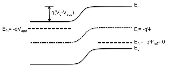
In this example to forward bias the diode, a positive voltage is applied to the Vcc contact, which is set equal to Qfn by the ohmic contact equations, while GND, which is equal to Qfp, is set to 0V (as seen in the tcl script below). The adjusted band diagram is represented in the figure below.
contact name=Vcc voltage supply=1.0
contact name=GND voltage supply=0.0
Give Initial Conditions:
sel z= {(Doping>0.0) ?  ( 0.025*log( (Doping+1.0e10) / 1.0e10))
:  (-0.025*log(-(Doping+1.0e10) / 1.0e10))} name = DevPsi
sel z=1.0e10*exp(DevPsi/0.025) name=Elec
sel z=1.0e10*exp(-DevPsi/0.025) name=Hole
sel z=0.0 name=Qfn
sel z=0.0 name=Qfp
Run the Simulation
device


